 Hitachi-HTDK185UK-mc-sm维修电路原理图.pdf
《Hitachi-HTDK185UK-mc-sm维修电路原理图.pdf》由会员分享,可在线阅读,更多相关《Hitachi-HTDK185UK-mc-sm维修电路原理图.pdf(48页珍藏版)》请在收音机爱好者资料库上搜索。
1、CAUTION: Before servicing this chassis, it is important that the service technician read the “Safety Precautions” and “Product Safety Notices” in this service manual. ATTENTION: Avant deffectuer lentretien du chassis, le technicien doit lire les Prcautions de scurit et les Notices de scurit du produ
2、it prsents dans le prsent manuel. VORSICHT: Vor ffnen des Gehuses hat der Service-Ingenieur die Sicherheitshinweise“ und Hinweise zur Produktsicherheit“ in diesem Wartungshandbuch zu lesen. SERVICE MANUAL MANUEL DENTRETIEN WARTUNGSHANDBUCH Data contained within this Service manual is subject to alte
3、ration for improvement. Les donnes fournies dans le prsent manuel dentretien peuvent faire lobjet de modifications en vue de perfectionner le produit. Die in diesem Wartungshandbuch enthaltenen Spezifikationen knnen sich zwecks Verbesserungen ndern. SPECIFICATIONS AND PARTS ARE SUBJECT TO CHANGE FOR
4、 IMPROVEMENT DVD AV Receiver and Digital Terrestrial TV Receiver October 2004 SM0154 HTD-K185UK RadioFans.CN 收音机爱 好者资料库 A) HARDWARE 1. GENERAL DESCRIPTION 1.1 MT1379 The MT1379 Progressive Scan DVD-Player Combo Chip is a single-chip MPEG video decoding chip that integrates audio/video stream data pr
5、ocessing, TV encoder, four video DACs with Macrovision, copy protection, DVD system navigation, system control and housekeeping functions. The features of this chip can be listed as follows; General Features: * Progressive scan DVD-player combo chip * Integrated NTSC/PAL encoder, * Built-in progress
6、ive video output * DVD-Video, VCD 1.1, 2.0, and SVCD, * Unified track buffer and A/V decoding buffer, * Direct interface of 32-bit SDRAM, * Servo controller and data channel processing. Video Related Features: * Macrovision 7.1 for NTSC/PAL interlaced video, * Simultaneous composite video and S-vide
7、o outputs, or composite and YUV outputs, or composite and RGB outputs. * 8-bit CCIR 601 YUV 4:2:2 output. * Decodes MPEG video and MPEG2 main profile at main level. * Maximum input bit rate of 15Mbits/sec. Audio Related Features: * Dolby Digital (AC-3) and Dolby Pro Logic * Dolby Digital S/PDIF digi
8、tal audio output * High-Definition Compatible Digital. (HDCD) decoding * Dolby Digital Class A and HDCD certified * SRS True Surround * CD-DA * MP3 RadioFans.CN 收音机爱 好者资料库 1.2 Memory SDRAM Memory Interface The MT1379 provides a glueless 16-bit interface to DRAM memory devices used as OSD, MPEG strea
9、m and video buffer memory for a DVD player. The maximum amount of memory support is 16 MB of Synchronous DRAM (SDRAM). The memory interface is configurable in depth to support 128-Mb addressing. The memory interface controls access to both external SDRAM memories, which can be the sole unified exter
10、nal read/write memory acting as program and data memory as well as various decoding and display buffers. 1.3 Drive Interfaces The MT1379 supports the DV34 interface, and other RF and servo interfaces used by many types of DVD loaders. These interfaces meet the specifications of many DVD loader manuf
11、acturers. 1.4 Front Panel The front panel is based around a Futaba VFD and a common NEC front panel controller chip, (uPD16311). The MT1379 controls the uPD16311 using several control signals, (clock, data, chip select). The infrared remote control signal is passed directly to the MT1379 for decodin
12、g. 1.5 Rear Panel A typical rear panel is included in the reference design. This rear panel supports: Six channel or two channel audio outputs, Optical and coax SPDIF outputs, Composite, S-Video, and SCART outputs. The six-video signals used to provide CVBS, S-Video, and RGB are generated by the MT1
13、379s internal video DAC, The video signals are buffered by external circuitry. Six channel audio output by the MT1379 in the form of three I2S (or similar) data streams. The S/PDIF serial stream is also generated by the MT1379 output by the rear panel. The six channel audio DACs (AK4356, PCM1606) ar
14、e used for six channel audio output with MT1379, and similarly AK4382A, CS4392 Audio DACs are used for two channel audio output with MT1379. 12-pin DDX board output jack gives out the amplified audio. Digital Audio is processed in the DDX-8228 IC and then amplified in the DDX-2050 Power Amplifier IC
15、s. 2. SYSTEM BLOCK DIAGRAM AND MT1379 PIN DECRIPTION 2.1 MT1379 Pin Description Pin Number Symbol Type Description 1 IREF Analog Input Current reference input. It generates reference current for data PLL. Connect an external 100K resistor to this pin and PLLVSS. 2 PLLVSS Ground Ground pin for data P
16、LL and related analog circuitry 3 LPIOP Analog Output Positive output of the low pass filter 4 LPION Analog Output Negative output of the low pass filter 5 LPFON Analog output Negative output of loop filter amplifier 6 LPFIP Analog Input Positive input of loop filter amplifier 7 LPFIN Analog Input N
17、egative input of loop filter amplifier 8 LPFOP Analog Output Positive output of loop filter amplifier 9 JITFO Analog Output RF jitter meter output 10 JITFN Analog Input Negative input of the operation amplifier for RF jigger meter 11 PLLVDD3 Power 3.3V power pin for data PLL and related analog circu
18、itry 12 FOO Analog Output Focus servo output. PDM output of focus servo compensator 13 TRO Analog Output Tracking servo output. PDM output of tracking servo compensator 14 TROPENPWM Analog Output Tray open output, controlled by microcontroller. This is PWM output for TRWMEN27hRW2=1 or is digital out
19、put for TRWMEN27hRW2=0 15 PWMOUT1 Analog Output The 1st general PWM output 16 PWMOUT2 Analog Output The 2nd general PWM output 17 DVDD2 Power 2.5V power pin for internal fully digital circuitry 18 DMO Analog Output Disk motor control output. PWM output 19 FMO Analog Output Feed motor control. PWM ou
20、tput 20 DVSS Ground Ground pin for internal fully digital circuitry 21 FG Input 1 Motor Hall sensor input 22 HIGHAO Inout 2-16 MA, SR PU Microcontroller address 8 23 HIGHA1 Inout 2-16 MA, SR PU Microcontroller address 9 24 HIGHA2 Inout 2-1 6MA, SR PU Microcontroller address 10 25 HIGHA3 Inout 2-16MA
21、, SR PU Microcontroller address 11 26 HIGHA4 Inout 2-16MA, SR PU Microcontroller address 12 27 HIGHA5 Inout 2-16MA, SR PU Microcontroller address 13 28 DVSS Ground Ground pin for internal digital circuitry 29 HIGHA6 Inout 2-16MA, SR PU Microcontroller address 14 30 HIGHA7 Inout 2-16MA, SR PU Microco
22、ntroller address 15 31 AD7 Inout 2-16MA, SR Microcontroller address/data 7 32 AD6 Inout 2-16MA, SR Microcontroller address/data 6 33 ADS Inout 2-16MA, SR Microcontroller address/data 5 34 AD4 Inout 2-16MA, SR Microcontroller address/data 4 35 DVDD3 Power 3.3V power pin for internal digital circuitry
23、 36 ADS Inout 2-16MA, SR Microcontroller address/data 3 37 AD2 Inout 2-16MA, SR Microcontroller address/data 2 38 AD1 Inout 2-16MA, SR Microcontroller address/data 1 39 ADO Inout 2-16MA, SR Microcontroller address/data 0 40 IOAO Inout 2-16MA, SR PU Microcontroller address 0 / IO 41 IOA1 Inout 2-16MA


- 配套讲稿:
如PPT文件的首页显示word图标,表示该PPT已包含配套word讲稿。双击word图标可打开word文档。
- 特殊限制:
部分文档作品中含有的国旗、国徽等图片,仅作为作品整体效果示例展示,禁止商用。设计者仅对作品中独创性部分享有著作权。
- 关 键 词:
- Hitachi HTDK185UK mc sm 维修 电路 原理图

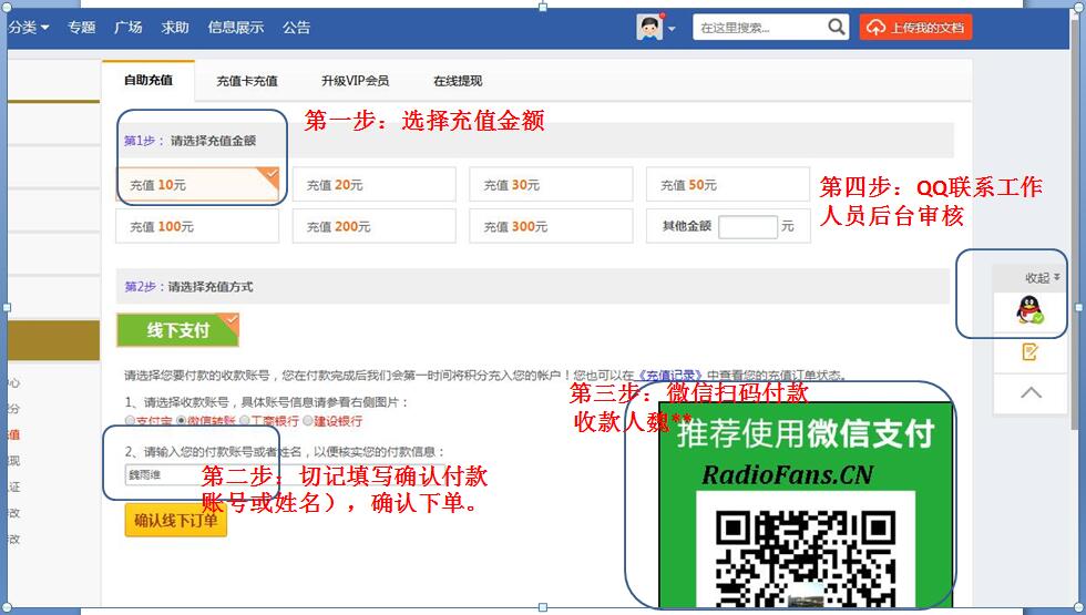
 收音机爱好者资料库所有资源均是用户自行上传分享,仅供网友学习交流,未经上传用户书面授权,请勿作他用。
 Marshall-9100-62-02-Schematic电路原理图.pdf
-
Marshall-4150-100W-Schematic电路原理图.pdf
-
Marshall-DBS-7200-72115-72410-200W-Head-7111-61-02-Schematic电路原理图.pdf
-
Marshall-5002-Schematic电路原理图.pdf
-
Marshall-5506-JCM800-Bass-30W-Schematic电路原理图.pdf
-
Marshall-DBS-7200-72115-72410-200W-Head-7111-60-0c-Schematic电路原理图.pdf
-
Marshall-1968-100W-Schematic电路原理图.pdf
-
Marshall-4501-50W-Power-Amp-Schematic电路原理图.pdf
-
Marshall-9001-4-Schematic电路原理图.pdf
-
Marshall-DLS201-Schematic电路原理图.pdf
-
Marshall-DBS-7200-72115-72410-200W-Head-7111-62-02-Schematic电路原理图.pdf
-
Marshall-1987-50W-Schematic电路原理图.pdf
-
Marshall-1987-Mk2-50W-Lead-Schematic电路原理图.pdf
-
Marshall-9100-65-02-Schematic电路原理图.pdf
-
Marshall-DBS-7200-72115-72410-200W-Head-7111-65-02-Schematic电路原理图.pdf
-
Marshall-2550-Amp-Schematic电路原理图.pdf
-
Marshall-4145-Schematic电路原理图.pdf
-
Marshall-5520-200W-Power-Amp-Bass-Combo-Schematic电路原理图.pdf
-
Marshall-2500SL-X-5881-2500-60-58-Issue-12-Schematic电路原理图.pdf
-
Marshall-5213-Power-Amp-Schematic电路原理图.pdf
-
Marshall-2555-Psu-Schematic电路原理图.pdf
-
Marshall-6100-6101-6100-61-04-Issue-4-Schematic电路原理图.pdf
-
Marshall-5502-Schematic电路原理图.pdf
-
Marshall-5503-JCM800-Bass-30W-Schematic电路原理图.pdf
-
Marshall-8040-Valvestate-Schematic电路原理图.pdf
-
Marshall-6100-6101-6100-65-04-Issue-6-Schematic电路原理图.pdf
-
Marshall-2100-SL-X-EL34-2100-60-34-issue10-Schematic电路原理图.pdf
-
Marshall-DBS-7400-400W-Head-7400-61-02-Schematic电路原理图.pdf
-
Marshall-DLS50-DL50-63-02-Schematic电路原理图.pdf
-
Marshall-2501-50W-Power-Amp-Schematic电路原理图.pdf
-
Marshall-3005H-12W-Lead-Schematic电路原理图.pdf
-
Marshall-3315-5150-Power-Amp-Schematic电路原理图.pdf
-
panasonic_rf-423_service.pdf
-
panasonic_rf-544_service.pdf
-
panasonic_rf-2200_service.pdf
-
panasonic_rf-4800_portable_radio_sm.pdf
-
panasonic_rf-b45.pdf
-
panasonic_rf-b60l_service_manual.pdf
-
panasonic_rf-b600_service.pdf
-
ITT 3214.pdf
-
ITT CX75.pdf
-
ITT RC500A.pdf
-
ITT RX75.pdf
-
ITT Synchrocompact 108.pdf
-
ITT_103.pdf
-
ITT_103SKJunior.pdf
-
ITT_109Tiny.pdf
-
ITT_200.pdf
-
ITT_6100.pdf
-
ITT_Junior28.pdf
-
ITT_Junior108.pdf
 Hitachi-D45S-tape-sm维修电路原理图.pdf
Hitachi-D707ll-tape-sm维修电路原理图.pdf
Hitachi-DA006-cd-sm维修电路原理图.pdf
Hitachi-D980M-tape-sm维修电路原理图.pdf
Hitachi-DE95-tape-sm维修电路原理图.pdf
Hitachi-HA2-int-sm维修电路原理图.pdf
Hitachi-D800U-tape-sm维修电路原理图.pdf
Hitachi-DA007-cd-sm维修电路原理图.pdf
Hitachi-DE99-tape-sm维修电路原理图.pdf
Hitachi-HA3-int-sm维修电路原理图.pdf
Hitachi-D45S-tape-sm维修电路原理图.pdf
Hitachi-D707ll-tape-sm维修电路原理图.pdf
Hitachi-DA006-cd-sm维修电路原理图.pdf
Hitachi-D980M-tape-sm维修电路原理图.pdf
Hitachi-DE95-tape-sm维修电路原理图.pdf
Hitachi-HA2-int-sm维修电路原理图.pdf
Hitachi-D800U-tape-sm维修电路原理图.pdf
Hitachi-DA007-cd-sm维修电路原理图.pdf
Hitachi-DE99-tape-sm维修电路原理图.pdf
Hitachi-HA3-int-sm维修电路原理图.pdf